There appears to be very little information on the web regarding the Prime 3B multiIO chip, so I took the opportunity to trace out the jumpers to the relevant control pins on the Prime 3B. This information should make it fairly easy for people with other cards based on the Prime 3B to work out their jumper assignments.
A text version of an earlier version of this document is also available.
7 June 2001: I have received some scanned pages from a manual for this card from Ian Hamilton. These have confirmed the jumper functionality I had deduced and have filled in the last remaining uncertainties. For those interested, Iain's scans of page 1 and page 2 are available, but note that these files are about 100K each.
13 March 2002: Derk Wachner mailed me to say that a card he has matches the above FCC ID and is manufactured by Kentech Computers, but it has a `Goldstar Prime 2C' (9413) chip on it. His card carries a warranty label of `4/94 KT 4863924'. It seems the FCC label does not uniquely identify a card based on a Prime3B chip; it would therefore be a good idea to double-check the chip used on a card before applying the information contained in this document.
For clarity, this is also available in postscript, fig and text versions.
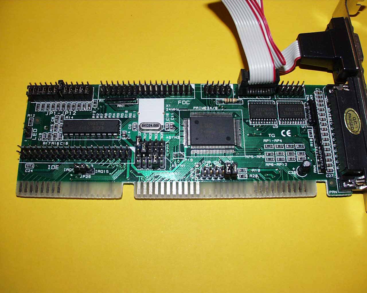
Photos of the component-side and solder-side of this board are also now available thanks to Ian Hamilton. These files are approximately 100K each. Note that on this board, the D-connector above the printer port plug is connected to serial port 1 whereas on my board it was the games port. The board pictured may be a slightly newer revision than mine since the board I worked with did not use surface-mount pullup resistors (they were mostly standard 1/4W types). However, in all other aspects including layout and jumper useage, the boards are identical.
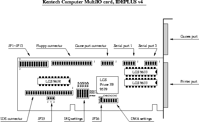
The LGS-9538 appears to handle the games port and perhaps takes a minor roll in the IDE port implementation.
The LGS-Prime3B seems to handle the address decoding, FDD control, most of the IDE functionality, RS232 control and the printer port.
The "LGS" chips perportedly come from LGE (LG electronics). LGE were formerly Goldstar. For this reason, the "Prime 2" chips for MultiIO cards were from Goldstar whereas the "Prime 3" and "Prime 4" chips are from LGE.
On the card at hand, JP2-12 had pin 1 tied to +5V and pin 3 tied to ground. Pin 2 went to the LGS-Prime3B chip. JP1 is dealt with below.
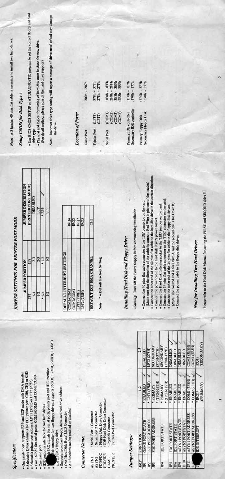
The JPs in the following table refer to this card; use this to cross reference the effects of +5V and ground on these pins.
| Function | JP | IC pin |
|---|---|---|
| Printer port select | 2 | Prime 3B #24 via discrete 4k7 resistor |
| FDD (port select) | 3 | Prime 3B #91 via 4k7 resistor |
| IDE (port select) | 4 | Prime 3B #92 via 4k7 resistor |
| FDD (enable) | 5 | Prime 3B #49 via 4k7 resistor |
| IDE (enable) | 6 | Prime 3B #50 via 4k7 resistor |
| Printer mode line #1 | 7 | Prime 3B #60 via 4k7 resistor |
| Printer mode line #2 | 8 | Prime 3B #57 via 4k7 resistor |
| Serial port 1 enable | 9 | Prime 3B #59 via 4k7 resistor |
| Serial port 2 enable | 10 | Prime 3B #51 via 4k7 resistor |
| Serial port 1 address | 11 | Prime 3B #64 via 4k7 resistor |
| Serial port 2 address | 12 | Prime 3B #63 via 4k7 resistor |
JP1 (game port enable) appears to be connected somewhat strangely:
For JP25, pin 1 was tied directly to pin C7 on the ISA bus while pin 3 was connected directly to pin C6 on the ISA bus.
Interrupts for the 2 serial ports and the printer port were selectable on this card between IRQs 3, 4, 5, 7 and 9. A jumper block matrix was used to switch the relevant pins from the Prime 3B to the ISA interrupt lines. Probing around this matrix revealed the Prime 3B pins used for this functionality:
For reference, the ISA bus locations of IRQs 3, 4, 5, 7 and 9 are B25, B24, B23, B21 and B4 respectively.
DMA usage for the printer port in ECP mode was selected with another block of jumpers, allowing a choice between DMA channels 0, 1 and 3. Two jumpers were required, one switching the DRQ to the Prime 3B, and the other taking care of the DAQ (DMA acknowledge). Once again, the Prime 3B pins used for this functionality were deducable:
For reference, the ISA bus pins of the req/ack signals for DMA 0, 1 and 3 are D9/D8, B18/B17 and B16/B15 respectively.
A final "jumper" was labeled JP26. (On Ian's board this "jumper" was labelled JP19 but was located in exactly the same place and is presumedly connected in the same way.) This had been soldered 1-2. Pin 1 was connected to ISA pin A21 which is the SA10 line (address bit 10). Pin 2 went to Prime 3B pin #96 and pin 3 was tied ground. Pin #96 on the Prime 3B obviously enables something when asserted and JP26 is used to select whether this is controlled by the SA10 address line or permanently held low. The actual purpose of this control line on the Prime 3B is at this point unknown.
The control lines for the LGS-9633 connected to Serial port 1 are located somewhere between pins 31 and 50 of the Prime 3B. For serial port 2, the drive lines are somewhere between Prime 3B pins 50 and 65. This vague information should allow serial port 1 and 2 to be identified.
Thanks are due to Ian Hamilton who provided photographs of his IO card. In addition, his provision of scanned copies of the original operating instructions (which I didn't have) has allowed the final gaps in this document to be filled in.
In addition, Peter made me aware of the existance of `printer only' versions of this card, which add further confirmation to the jumper assignments detailed herein.
Jonathan Woithe
13 March 2001
Revised: 7 June 2001, 29 August 2001, 13 march 2002